 TFStudio
 Reading the Admittance Diagram
What the admittance locus plots, why every dielectric layer draws a circle, and three coatings read off the diagram in TFStudio.
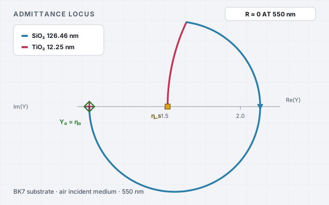
A reflectance curve says what a coating does. It does not say how the coating gets there, or which layer is responsible. The admittance diagram answers that: it draws the state of the stack layer by layer, at one wavelength, as a path in the complex plane.
Everything below uses built-in material data so the numbers can be reproduced exactly.
What the diagram plots
Take the characteristic matrix of the layers between the substrate and the point you have reached, apply it to the substrate, and you get the pair that carries all the information about the assembly:
The surface admittance is their ratio:
That single complex number is what the diagram plots. Reflectance follows from it and nothing else:
Admittances are given in units of the admittance of free space, so at normal incidence they take the same numerical values as the refractive indices. The substrate sits at , air sits at .
The path starts at the substrate and moves outward, one arc per layer. Where it finishes is , and how far that endpoint sits from is the reflectance. Nothing else about the path matters to , but the path is what tells you which layer to change.
Why every dielectric layer draws a circle
Write and let the layer start from admittance . For a dielectric layer, and are both real, and eliminating from the transfer relation gives
This is a circle centred on the real axis, passing through its own starting point, and traced clockwise as the layer grows.
Four consequences do most of the work when reading a diagram:
- The two points where a layer's circle crosses the real axis always multiply to .
- A quarter-wave layer is exactly half a circle: it maps a real admittance to .
- A half-wave layer is a full circle back to the starting point: the absentee layer, seen geometrically.
- An absorbing layer has complex and , so its locus is a spiral that does not close.
Opening it in TFStudio
Open Analysis → Admittance (documentation).
The panel on the left sets Wavelength, AOI, Polarization, Side, and the drawing Plane. Use for the admittance locus and for the same information mapped into the reflection plane, where the endpoint radius is and the whole picture stays inside the unit circle.
Three points are marked on the chart:
- η_s, a yellow square: the substrate, where the path begins.
- η₀, a red cross: the incident medium, the target for any antireflection coating.
- Y₀, a green diamond: where the path actually ends.
Each arc is one layer, coloured by material, with a dot at its outer end. The table below the chart lists the admittance and reflection coefficient at every boundary, reading from the substrate outward. Note that the arcs are numbered from the incident medium inward, so L1 is the layer touching air, which is the opposite of the Design Editor's numbering.
One quarter-wave layer
Build Air | MgF2 99.75 nm | BK7 with the built-in data at 550 nm:
| Catalog entry | at 550 nm |
|---|---|
MgF2 |
1.378506 |
BK7 (Schott) |
1.518522 |
A quarter wave is nm. The diagram shows one semicircle, starting on the real axis at the substrate and dipping below it before returning to the axis:
The two real-axis crossings, 1.51852 and 1.25140, multiply to 1.900278, which is for MgF₂. That is the circle rule, checked on the readout.
The endpoint is closer to than the bare substrate was, so the reflectance falls from 4.2388% to 1.2469%. It stops short of because landing exactly on it would need
and no durable coating material has that index. The gap between 1.25140 and 1 on the diagram is the residual reflectance of a single-layer AR coating.
Double the thickness to 199.49 nm and the locus closes into a full circle back onto : returns to 4.2388%, the half-wave absentee.
A quarter-wave mirror
Now the opposite case. Build (HL)^4 with Design → Formula, H = TiO2, L = SiO2 (Fused Silica), substrate BK7 (Schott), reference 550 nm, which gives nm and nm.
Every layer is a quarter wave, so every arc is a half-circle that starts and ends on the real axis. High-index layers arc above it, low-index layers below, and each endpoint is divided by the previous one:
| Boundary | if the stack stopped here | |
|---|---|---|
| η_s (BK7) | 1.51852 | 4.24% |
| after L8 (SiO₂) | 1.40356 | 2.82% |
| after L7 (TiO₂) | 4.51230 | 40.60% |
| after L6 (SiO₂) | 0.47234 | 12.84% |
| after L5 (TiO₂) | 13.40833 | 74.17% |
| after L4 (SiO₂) | 0.15896 | 52.66% |
| after L3 (TiO₂) | 39.84296 | 90.45% |
| after L2 (SiO₂) | 0.05349 | 80.72% |
| after L1 (TiO₂) | 118.39364 | 96.68% |
Each HL pair multiplies the admittance by
which is the whole mirror in one number: the path hops further from with every pair, alternating between very large and very small real values. Sixteen layers reach and ; thirty-two layers reach and .
This is the design where the default framing gets in the way. The view is scaled to the substrate and incident-medium admittances, so the outer arcs of a long stack run far outside it. Zoom out to follow them, or switch the Plane control to , which stays bounded no matter how large becomes. In the plane the same endpoint sits at , a radius of 0.98325 from the origin, and .
Landing exactly on η₀
A two-layer V-coat puts the endpoint on itself. With the same built-in TiO₂ and SiO₂ on BK7, solving at 550 nm gives
The path is two arcs:
| Boundary | |
|---|---|
| η_s (BK7) | |
| after the TiO₂ layer | |
| after the SiO₂ layer |
The thin titania layer only lifts the admittance off the real axis. All the work is done by the silica layer, and it works because of where its circle happens to lie: centred at 1.5657 with radius 0.5658, so it crosses the real axis at 0.9999 and 2.1316, and those two intercepts multiply to 2.1313, which is for silica.
That is the whole design condition, stated geometrically: the outermost layer's circle has to pass through , and the layer has to be thick enough to get there. The titania thickness exists only to place the start of that circle correctly.
Change the wavelength and the endpoint walks away from :
| λ | |||
|---|---|---|---|
| 500 nm | 0.1979 | 0.99% | |
| 550 nm | 0.0001 | 0.00% | |
| 600 nm | 0.1482 | 0.52% | |
| 650 nm | 0.2639 | 1.51% |
Both arcs change length with wavelength, because the phase thickness does. That is why a V-coat is narrow. Push far enough to the blue and it stops helping at all: at 450 nm this design reflects 5.41%, against 4.33% for uncoated BK7.
Conventions worth knowing
- The diagram is drawn at one wavelength and one angle at a time. A locus says nothing about the rest of the spectrum.
- At oblique incidence the layers are entered by their tilted admittances, and , with from Snell's law. The s and p loci separate, and itself moves, so the target the coating has to reach is not where it was at normal incidence.
- Loci are traced clockwise, following Macleod's orientation.
- The built-in MgF₂, SiO₂ and TiO₂ datasets have across the visible, so every arc in these examples is a true circle. With real absorbing data the arcs become spirals, and a coating can no longer return exactly to where it started.
References
- H. A. Macleod, Thin-Film Optical Filters, 5th ed. Equation 2.113 for the characteristic matrix of an assembly, Equations 3.3–3.5 and Figure 3.1 for the admittance locus, its clockwise circle and the isoreflectance contours, and §9.2 for tilted admittances at oblique incidence.
- Admittance Diagram for the window's settings and readouts.