 TFStudio
 Designing a Two-Layer V-Coat for 550 nm
Design a two-layer V-coat on N-BK7 with SiO2 and ZrO2, solve both thicknesses for zero reflectance at 550 nm, and check the minimum in TFStudio.
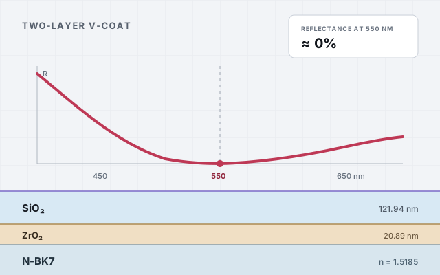
A single MgF₂ layer on N-BK7 gets the front-surface reflectance down to about 1.25% at 550 nm. A two-layer V-coat can place a much deeper minimum at one wavelength.
This design uses SiO₂ and ZrO₂ on N-BK7. It is meant for normal incidence and a design wavelength of 550 nm.
What a V-coat does
The name comes from the reflectance plot: the curve falls toward a narrow minimum and rises again on either side.
With one layer, only one thickness can move. With two layers, there are two thickness variables. At a single wavelength they can drive both parts of the complex reflection amplitude to zero:
This does not make the coating broadband. It gives a deep minimum around the wavelength used for the calculation.
Material values at 550 nm
Use these specific entries from the coating-material library:
SiO2 (110-800nm, RIT):ZrO2 (190-800nm, RIT):- N-BK7 substrate:
- Air:
The exact catalog entry matters. Another ZrO₂ dataset can have a different index and extinction coefficient, so it will produce different thicknesses.
Why two quarter-wave layers are not enough
A quarter-wave starting thickness for each material would be
Quarter-wave phase by itself is not enough. A quarter-wave layer transforms the optical admittance on its far side. For the physical order air / SiO₂ / ZrO₂ / N-BK7, with ZrO₂ touching the substrate, the two ideal lossless quarter-wave transformations give
There is zero reflection only when the transformed admittance matches air:
For these materials,
Those ratios do not match. Using the real indices gives and therefore
The full TMM calculation, including the ZrO₂ extinction coefficient, gives 3.33%. Fixing both layers at one quarter wave fixes both phase thicknesses, so there is no remaining variable to correct this admittance mismatch. Moving the two thicknesses away from quarter wave lets them drive both and to zero.
The 550 nm design
Here is the calculation used to obtain the thicknesses. At normal incidence, the phase thickness and characteristic matrix of layer are
The complex index is used directly here; the extinction coefficient is not discarded. For the physical order SiO₂ then ZrO₂, the total matrix is . TFStudio then calculates
The two unknowns are and . I searched the first half-wave interval for each layer,
using several starting points, then used a two-variable Newton solve for
The compact root converges to
There is another root in the same search interval, near 66.36 nm of SiO₂ and 105.96 nm of ZrO₂. The solution used here has the smaller total thickness and much less absorbing ZrO₂.
Rounded to practical values, the design is:
The physical stack is
With the thicknesses rounded to two decimal places, the calculated front-surface reflectance at 550 nm is about , which will normally display as zero.
The selected ZrO₂ data has a nonzero extinction coefficient. At the design wavelength the same model gives approximately
So the reflected power is nearly zero, but a small amount is absorbed.
Building it in TFStudio
1. Set the design geometry
- Reference wavelength: 550 nm
- Incident medium: Air
- Substrate: N-BK7
2. Add the two layers
The physical order from air to substrate is:
SiO2 (110-800nm, RIT): 121.94 nmZrO2 (190-800nm, RIT): 20.89 nm
The Design Editor lists the substrate-adjacent layer first. Enter ZrO₂ first in the table, then SiO₂.

3. Check the spectrum
Run a thickness refinement, then plot reflectance over 400–700 nm. The expected front-surface values are approximately:
- 500 nm: 0.91%
- 550 nm: 0%
- 600 nm: 0.52%
- 650 nm: 1.54%
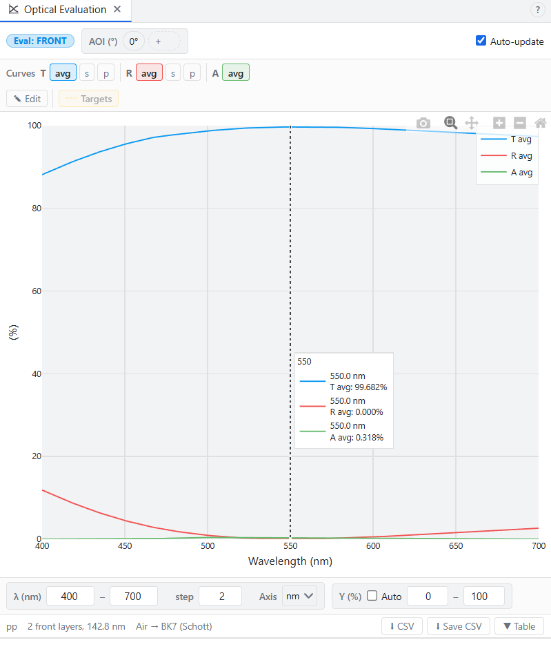
The minimum is narrow and the two sides are not perfectly symmetric because the material indices are dispersive.
What to keep in mind
- This is a normal-incidence, single-wavelength design.
- Changing either catalog entry changes the result.
- Zero reflectance does not mean zero absorption.
- Thickness errors move the minimum and raise its floor.
For a wider low-reflectance band, two layers are usually not enough; that is a different optimization problem.