 TFStudio
 Refining a Four-Layer Broadband AR Coating
Set a 450–650 nm antireflection target in the Merit Function Editor and refine a four-layer MgF2, HfO2, and SiO2 coating on BK7 with Refinement.
The first two tutorials used thicknesses calculated outside TFStudio and then checked the result. This time TFStudio will calculate the thicknesses.
The task is to reduce the front-surface reflectance of BK7 over 450–650 nm. We will start with a reasonable but poor four-layer coating, define what the optimizer should minimize, and run a thickness refinement. The number and order of the layers will stay fixed.
The design conditions
Use the following conditions throughout the example:
- Incident medium: Air
- Substrate: BK7 (Schott)
- Coated surface: Front
- Evaluation: Ignore other side
- Angle of incidence: 0°
- Polarization: Average
- Reference wavelength: 550 nm
- Optimization band: 450–650 nm
This is a calculation for one coated surface, not a complete glass plate with two reflecting surfaces.
Use these entries from the built-in material catalog. Their values at 550 nm are:
| Catalog entry | ||
|---|---|---|
MgF2 |
1.378506 | 0 |
HfO2 |
2.011238 | |
SiO2 (Fused Silica) |
1.459911 | 0 |
BK7 (Schott) |
1.518522 |
The material names matter because another catalog entry can use different dispersion or extinction data.
Build the starting coating
The physical order, read from the incoming air toward the substrate, is
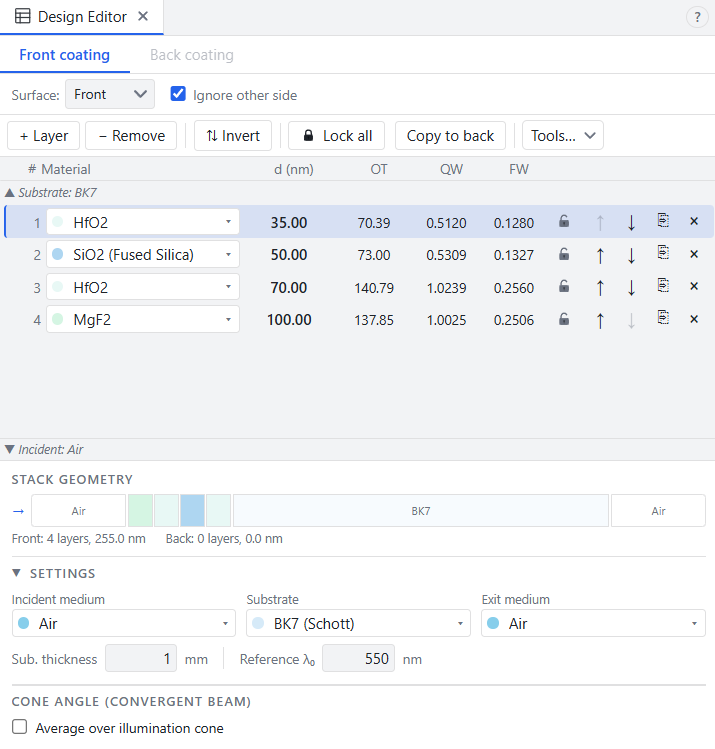
The 100 nm MgF₂ and 70 nm HfO₂ layers are close to quarter-wave thicknesses at 550 nm. The two thinner layers give the refiner two more phase adjustments. It is only a starting point; it is not expected to meet the broadband target.
The Design Editor lists the substrate-adjacent layer first. Enter the same stack in this order:
| Design Editor layer | Material | Starting thickness |
|---|---|---|
| 1 | HfO2 |
35 nm |
| 2 | SiO2 (Fused Silica) |
50 nm |
| 3 | HfO2 |
70 nm |
| 4 | MgF2 |
100 nm |
Leave all four thicknesses unlocked.
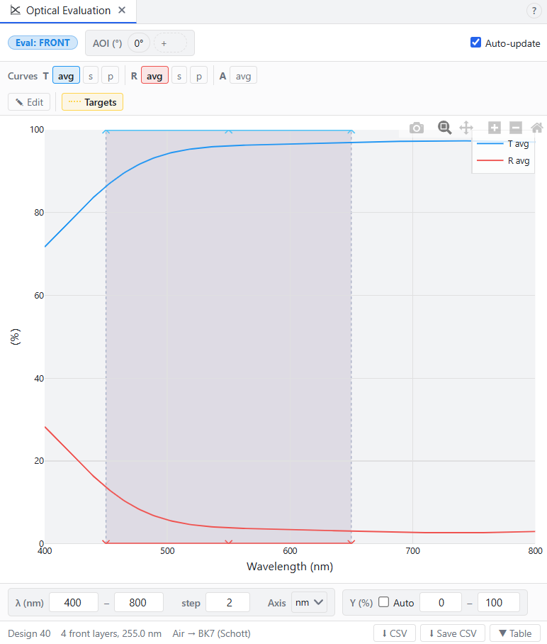
Before refinement, the average reflectance over 450–650 nm is 5.148%. The worst point is 13.66% at 450 nm, so the starting stack is not a broadband AR coating yet.
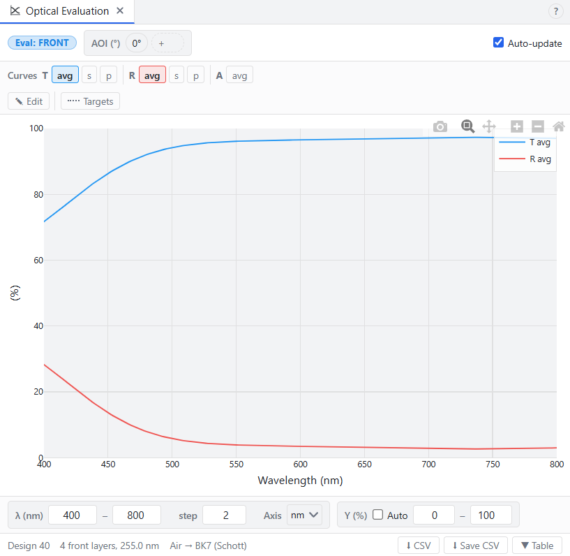
To calculate values mentioned above you can add a monitor in the bottom left corner of the program:

After clicking 'Add' you will see the average value of R over specified 450-650 nm range.

Define the merit function
A single-wavelength target such as would allow the optimizer to make another narrow V-coat. We instead need every sampled wavelength in the band to affect the result.

and use the filter-type wizard:
- Choose AR → Broadband AR.
- Set the wavelength range to 450–650 nm.
- Choose a continuous target.
- Set the angle to 0° and polarization to Average.
- Generate the operands.
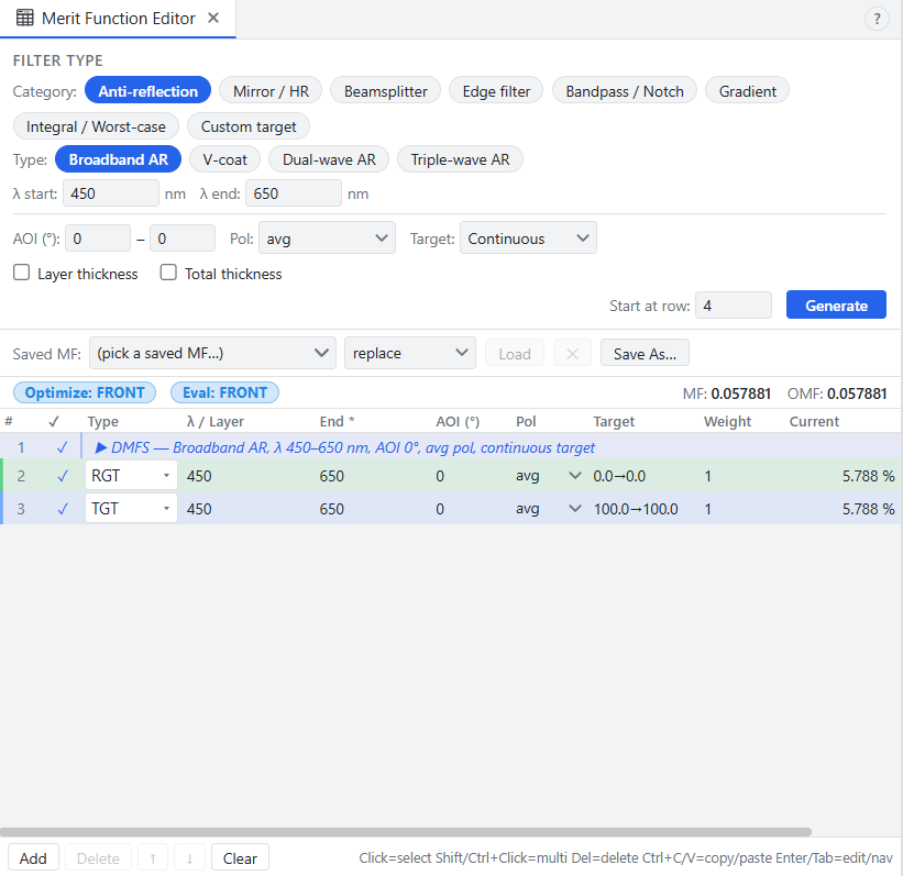
The wizard creates two equal-weight optical operands:
| Operand | Band | Target | Weight |
|---|---|---|---|
RGT |
450–650 nm | 1 | |
TGT |
450–650 nm | 1 |
RGT is the root-mean-square deviation of reflectance from zero over the band.
TGT does the same for transmission relative to one. Using both matters when layer's material contains extinction coefficients: a coating should not satisfy an AR target by absorbing the light instead of transmitting it.
The optical merit function is
where and are the two band RMS errors. OMF is a dimensionless error, not the average reflectance.
Add these thickness constraints in the same editor:
| Operand | Layers | Target |
|---|---|---|
MNT |
1-4 | 30 nm minimum |
MXT |
1-4 | 250 nm maximum |
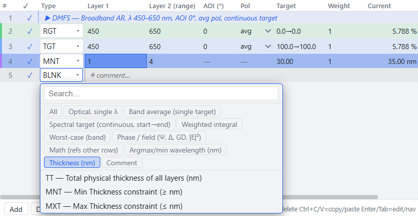
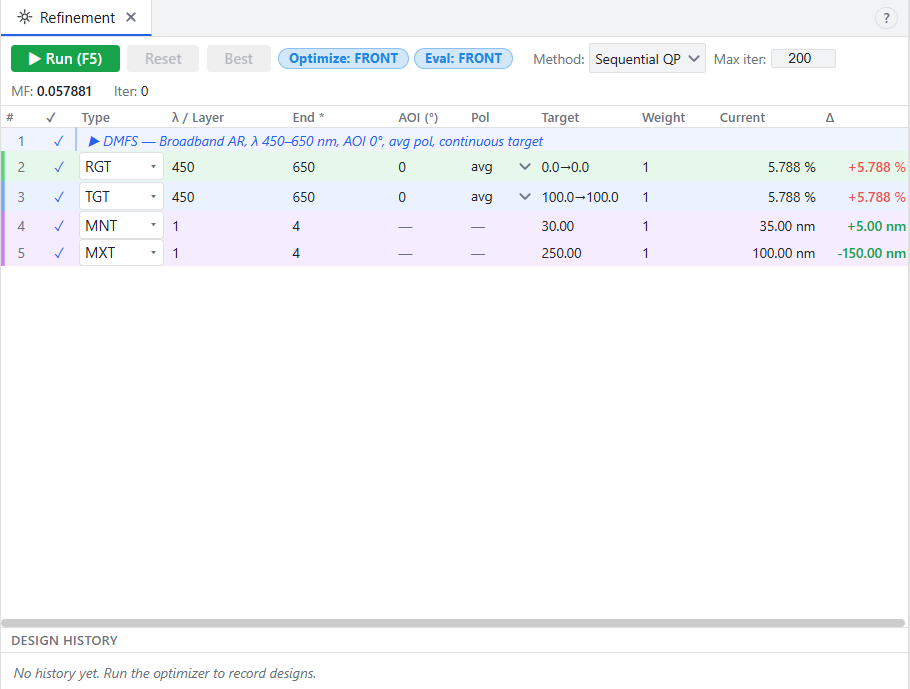
The limits keep the local refiner away from vanishingly thin or unnecessarily thick layers. Because the starting stack satisfies both limits, its total merit function (MF) value and optical-only merit function value (OMF) are equal: 0.057881.
You'll notice on the Optical Evaluation plot that region that is affected by set optical targets is now highlighted:
Run the refinement
Open Refinement

and use:
- Method: Sequential QP
- Maximum iterations: 200
Click Run. In this case it converges after 35 iterations and the resulting MF is 0.001014.
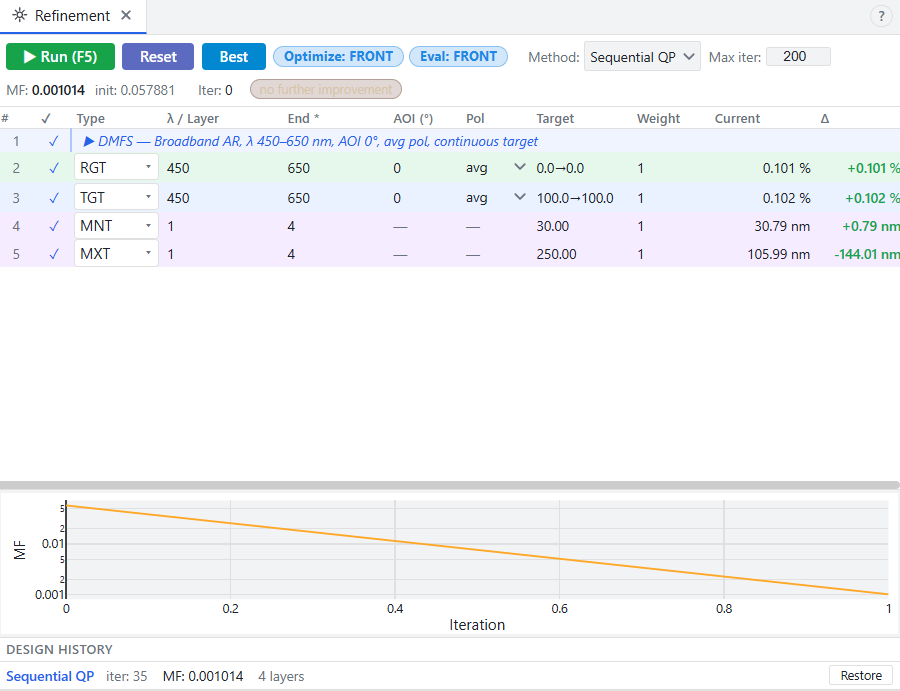
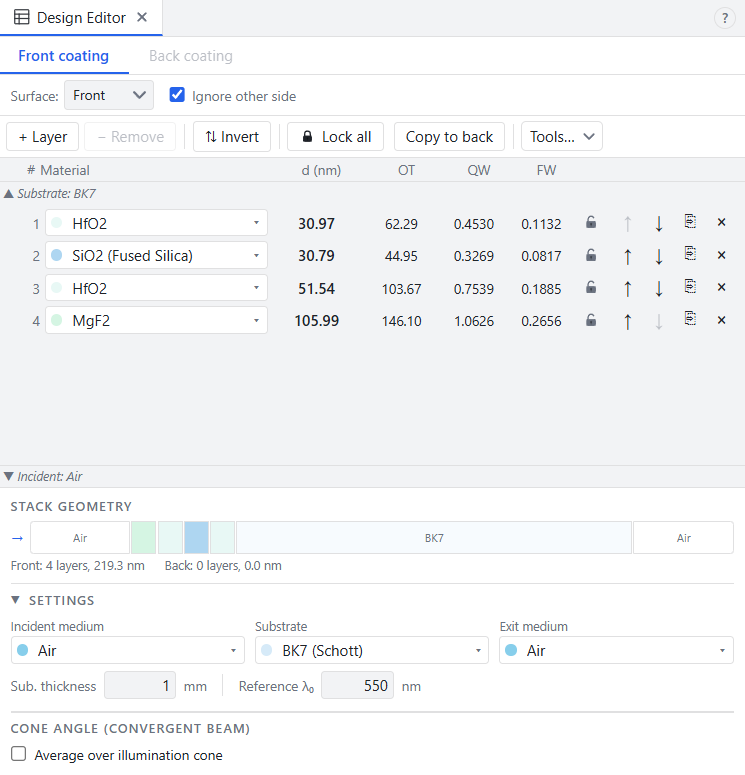
The resulting Design Editor table is:
| Layer | Material | Start | Refined |
|---|---|---|---|
| 1 | HfO2 |
35.00 nm | 30.97 nm |
| 2 | SiO2 (Fused Silica) |
50.00 nm | 30.79 nm |
| 3 | HfO2 |
70.00 nm | 51.54 nm |
| 4 | MgF2 |
100.00 nm | 105.99 nm |
The total coating thickness is 219.28 nm, and the thinnest layer is 30.79 nm.
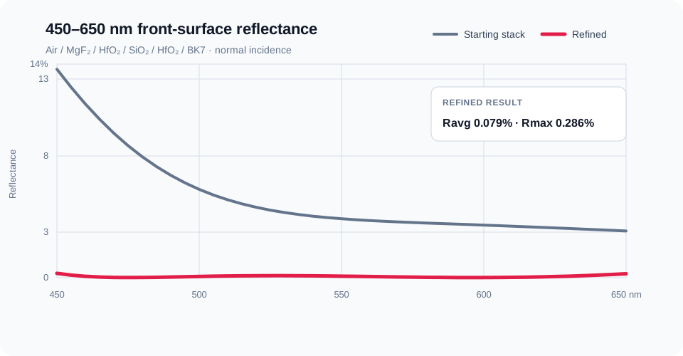
Compare the spectra
The plot uses the same wavelength range and vertical scale for both designs.
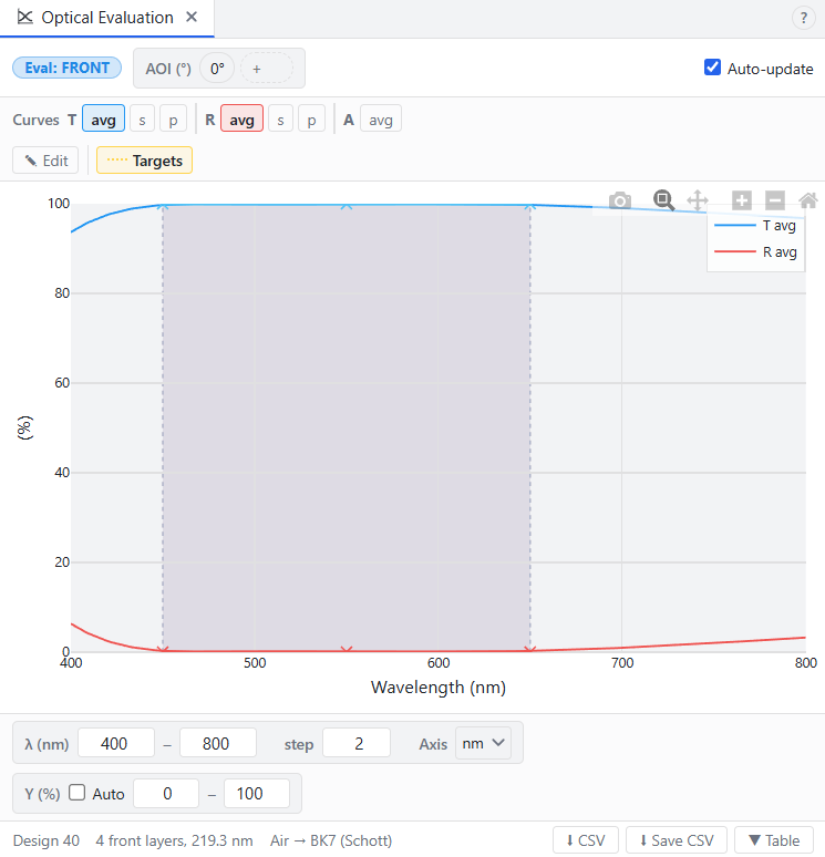
The refined curve sits close to the bottom of the plot, so the table below gives its values more clearly.
| Wavelength | Starting | Refined | Refined |
|---|---|---|---|
| 450 nm | 13.6634% | 0.2858% | 99.7138% |
| 500 nm | 5.7872% | 0.0791% | 99.9204% |
| 550 nm | 3.8629% | 0.0995% | 99.8999% |
| 600 nm | 3.4452% | 0.0084% | 99.9909% |
| 650 nm | 3.0635% | 0.2546% | 99.7445% |
Checked on a 1 nm grid from 450 to 650 nm:
| Metric | Starting design | Refined design |
|---|---|---|
| Average reflectance | 5.148% | 0.08% |
| Maximum reflectance | 13.663% | 0.286% |
| MF / OMF | 0.057881 | 0.001014 |
| Total thickness | 255.00 nm | 219.28 nm |
What refinement did and did not do
Refinement moved four existing interfaces. It did not choose the materials, change their order, or add another layer. A different starting stack can settle into a different local minimum, so this result is not proof of a globally best four-layer design.
The result also applies only to the stated material data, one coated surface, normal incidence, and the 450–650 nm band. It has not yet been checked for oblique incidence, polarization splitting, or thickness errors. Those are separate analysis and tolerance problems.